

Transistor Level Design Electric Layout Tool
MOST CAD SYSTEMS use two methods to do circuit design: connectivity and geometry.
- The connectivity approach is used by every Schematic design system: you place components and draw connecting wires. The components remain connected, even when they move.
- The geometry approach is used by most Integrated Circuit (IC) layout systems: rectangles of "paint" are laid down on different layers to form the masks for chip fabrication.
ELECTRIC IS DIFFERENT because it uses connectivity for all design, even IC layout. This means that you place components (MOS transistors, contacts, etc.) and draw wires (metal-2, polysilicon, etc.) to connect them. The screen shows the true geometry, but it knows the connectivity too.
The advantages of connectivity-based IC layout are many:
- No node extraction. Node extraction is not a separate, error-prone step. Instead, the connectivity is part of the layout description and is instantly available. This speeds up all network-oriented operations, including simulation, layout-versus-schematic (LVS), and electrical rules checkers.
- No geometry errors. Complex components are no longer composed of unrelated pieces of geometry that can be moved independently. In paint systems, you can accidentally move the gate geometry away from a transistor, thus deleting the transistor. In Electric, the transistor is a single component, and cannot be accidentally destroyed.
- More powerful editing. Browsing the circuit is more powerful because the editor can show the entire network whenever part of it is selected. Also, Electric combines the connectivity with a layout constraint system to give the editor powerful manipulation tools. These tools keep the design well-connected, even as the circuit is modified on different levels of hierarchy.
- Tools are smarter when they can use connectivity information. For example, the Design Rule checker knows when the layout is connected and uses different spacing rules.
- Simpler design process. When doing schematics and layout at the same time, getting a correct LVS typically involves many steps of design rule cleaning. This is because node extraction must be done to obtain the connectivity of the IC layout, and node extractors cannot work when the design rules are bad. So, each time LVS problems are found, the layout must be fixed and made DRC clean again. Since Electric can extract connectivity for LVS without having perfect design rules, the first step is to get the layout and schematics to match. Then the design rules can be cleaned-up without fear of losing the LVS match.
- Common user interface. One CAD system, with a single user interface, can be used to do both IC layout and schematics. Electric tightly integrates the process of drawing separate schematics and has an LVS tool to compare them.
The disadvantages of connectivity-based IC layout are also known:
- It is different from all the rest and requires retraining. This is true, but many have converted and found it worthwhile. Users who are familiar with paint-based IC layout systems typically have a harder time learning Electric than those with no previous IC design experience.
- Requires extra work on the user's part to enter the connectivity as well as the geometry. While this may be true in the initial phases of design, it is not true overall. This is because the use of connectivity, early in the design, helps the system to find problems later on. In addition, Electric has many power tools for automatically handling connectivity.
- Design is not WYSIWYG (what-you-see-is-what-you-get) because objects that touch on the screen may or may not be truly connected. Electric has many tools to ensure that the connectivity has been properly constructed.
The way that Electric handles all types of circuit design is by viewing it as a collection of nodes and arcs, woven into a network.
| The nodes are electrical components such as transistors, contacts, and logic gates. Arcs are simply wires that connect two components. Ports are the connection sites on nodes where the wires connect. | 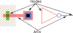 |
In the above example, the transistor node on the left has three pieces of geometry on different layers: polysilicon, active, and well. This node can be scaled, rotated, and otherwise manipulated without concern for specific layer sizes. This is because rules for drawing the node have been coded in a technology, which describes nodes and arcs in terms of specific layers.
Because Electric uses nodes and arcs for design, it is important that they be used to make all of the relevant connections. Although layout may appear to be connected when two components touch, a wire must still be used to indicate the connectivity to Electric. This requires a bit more effort when designing a circuit, but that effort is paid back in the many ways that Electric understands your circuit.
Besides creating meaningful electrical networks, arcs which form wires in Electric can also hold constraints. A constraint helps to control geometric changes, for example, the rigid constraint holds two components in a fixed configuration while the rest of the circuit stretches. These constraints propagate through the circuit, even across hierarchical levels of design, so that very complex circuits can be intelligently manipulated.
A cell is a collection of these nodes and arcs, forming a circuit description. There can be different views of a cell, such as the schematic, layout, icon, etc. Also, each view can have different versions, forming a history of design. Multiple views and versions of a cell are organized into Cell groups.
For example, a clock cell may consist of a schematic view and a layout view. The schematic view may have two versions: 1 (older) and 2 (newer). In such a situation, the clock cell group contains 3 cells: the layout view called "clock{lay}", the current schematic view called "clock{sch}", and the older schematic view called "clock;1{sch}". Note that the semicolon and numeric version number (;2) are omitted from the newest version.
Hierarchy is implemented by placing instances of one cell into another. When this is done, the cell that is placed is considered to be lower in the hierarchy, and the cell where it is placed is higher. Therefore, the notion of going down the hierarchy implies moving into a cell instance, and the notion of going up the hierarchy implies popping out to where the cell is placed. Note that cell instances are actually nodes, just like the primitive transistors and gates. By defining exports inside of a cell, these become the connection sites, or ports, on instances of that cell.
A collection of cells forms a library, and is treated on disk as a single file. Because the entire library is handled as a single entity, it can contain a complete hierarchy of cells. Any cell in the library can contain instances of other cells. A complete circuit can be stored in a single library, or it can be broken up into multiple libraries.
 | Previous |  | Table of Contents | Next |  |
Transistor Level Design Electric Layout Tool
Source: https://www.staticfreesoft.com/jmanual/mchap01-06.html
Posted by: thillsithems.blogspot.com
0 Response to "Transistor Level Design Electric Layout Tool"
Post a Comment